
A protected DC input for an industrial SBC must do more than convert 24 V to 12 V or 5 V. It has to survive wiring mistakes, control inrush current, keep transients away from the converter, and make brownouts predictable enough for the operating system to recover.
The right circuit depends on the installation and the product standard. A 24 V rail inside a short, controlled cabinet is different from a cable that runs outdoors or alongside motor wiring. Do not copy a surge level or TVS part number from a reference design without checking the coupling method, source impedance, grounding, and acceptance criteria for the final product.
A Useful Industrial DC Input Block
field connector
    -> fuse or current protection
    -> reverse-polarity / reverse-current stage
    -> surge and EFT clamp
    -> EMI filter
    -> inrush control / eFuse
    -> wide-input DC/DC converter
    -> hold-up and power-fail detection
    -> SBC rails
Not every product needs a separate device for every block. An integrated eFuse may combine several functions. The sequence is still useful because it forces the design review to account for each failure mode.
Start with the Disturbance Table
| Event | Typical cause | Desired system response |
|---|---|---|
| Reverse polarity | Field wiring error | No damage; no unsafe current |
| Overcurrent or short | Failed SBC, cable, or peripheral | Limit or disconnect without overheating |
| Inrush current | Charging bulk capacitance | Controlled ramp; upstream supply stays stable |
| Overvoltage | Wrong supply or regulator fault | Clamp or disconnect before downstream damage |
| Surge | Switching or lightning-related transient | Survive defined test; recover as specified |
| EFT/burst | Relay and contactor switching | No reset, corruption, or unsafe output |
| Brownout | Shared rail dip or cable loss | Continue briefly or shut down cleanly |
| Reverse current | Hold-up capacitor or alternate supply | Do not back-feed the field rail |
Write the pass behavior next to the test. “Survive” can mean uninterrupted operation, automatic recovery, or simply no damage. Those are different acceptance criteria.
Define the Real Voltage Window
The nominal label is not the design window. For a nominal 24 V system, document:
- minimum voltage during normal operation
- maximum continuous voltage
- cold-start and cable-drop conditions
- transient amplitude and duration
- upstream supply current limit
- input cable length and impedance
- chassis and signal-ground arrangement
A converter marked “9–36 V” may cover normal operation while having too little absolute-maximum margin after a TVS clamps a surge. Work backward from the downstream absolute maximum, including tolerances and temperature.
| Parameter | Example design entry | Where it comes from |
|---|---|---|
| Nominal input | 24 V DC | Cabinet power architecture |
| Normal operating range | Project-specific | Supply tolerance and cable drop |
| Required transient test | Project-specific | Product standard and installation |
| Maximum SBC load | Measured, not nameplate only | Boot plus CPU, storage, modem, USB |
| Allowed interruption | Application-specific | Filesystem and process behavior |
| Recovery behavior | Automatic or supervised | System safety requirement |
The example values belong in a project specification. They should not be inferred from the SBC connector label.
Reverse-Polarity Protection Options
Series Diode
A series diode is simple and predictable. Its drawbacks are voltage drop and heat. At several amperes, even a Schottky diode can consume meaningful thermal budget.
P-Channel MOSFET
A high-side P-channel MOSFET reduces voltage drop compared with a diode. The gate network must be checked for maximum gate voltage, turn-on behavior, surge exposure, and reverse current.
N-Channel MOSFET with Controller
An ideal-diode or eFuse controller can drive N-channel MOSFETs for lower loss and more complete protection. Integrated solutions may add current limiting, overvoltage cutoff, inrush control, diagnostics, and reverse-current blocking.
| Approach | Loss | Complexity | Useful when |
|---|---|---|---|
| Series diode | Highest | Low | Low current, generous voltage margin |
| P-channel MOSFET | Low | Medium | Moderate current and compact design |
| Controller/eFuse | Lowest to low | Medium | Higher current or multiple protection requirements |
Check failure behavior as carefully as normal efficiency. A component that fails short may keep the system running but remove protection without any indication.
TVS Selection Is an Energy Problem
A transient-voltage suppressor should remain off at the highest continuous input, clamp below the protected circuit’s safe voltage, and absorb the test-pulse energy without exceeding its rated junction condition.
The three voltages to keep separate are:
- standoff voltage: where the TVS should not conduct significantly
- breakdown voltage: where avalanche begins under a specified current
- clamping voltage: the voltage reached at a much larger pulse current
The clamping voltage—not the part number printed on the TVS—must fit below the downstream absolute maximum with margin. Add the effect of trace inductance. A long loop between connector, TVS, and return can create a damaging local spike even if the TVS is correctly rated.
Place the clamp close to the entry connector and give the pulse current a short, wide return path. Keep it away from sensitive ground references. Layout is part of the protection circuit.
Fuse and Current Limiting
A fuse mainly protects wiring and prevents sustained fault energy. It may be too slow to protect a semiconductor during a short circuit. An eFuse or hot-swap stage reacts faster and can set a repeatable current limit.
Coordinate the layers:
- The upstream supply should tolerate the planned inrush.
- The electronic current limit should allow legitimate boot and peripheral peaks.
- The fuse should clear faults that the electronic protection cannot safely hold forever.
- PCB traces and connectors must carry the fault current until protection operates.
Measure the real load waveform. LTE modems, USB devices, display backlights, and NVMe drives can produce peaks that a steady-state power estimate misses.
Input Filtering Without Creating a New Problem
An LC or pi filter can reduce conducted noise, but a lightly damped filter can ring when hit by a transient or interact with the DC/DC converter’s input impedance. That can produce an overvoltage after the original pulse is gone.
During design review, check:
- component saturation current
- capacitor DC-bias derating
- damping across operating conditions
- converter stability requirements
- conducted emissions and immunity in both cable polarities
- leakage paths to chassis or protective earth
A ferrite bead selected from a 100 MHz impedance plot may do little at a switching converter’s fundamental frequency. Use impedance data over the actual noise spectrum.
Inrush and Hot-Plug Behavior
The input capacitance looks like a short circuit at connection. The rough first-order charge is:
Q = C × ΔV
The peak current is set by source impedance, cable inductance, capacitor ESR, and any controlled ramp. It is not adequately described by average power.
Test hot plug with the longest and shortest expected cables and with the upstream supply at its maximum voltage. Watch both the product input and the shared rail. A design can boot correctly while causing every neighboring device on the rail to reset.
Brownout, Hold-Up, and Linux
More capacitance is not automatically better. It increases inrush, occupies space, and can leave the processor operating in an undefined voltage region for longer. Decide whether the product should ride through the disturbance or shut down quickly.
For a first estimate of hold-up capacitance under roughly constant current:
C ≈ I × Δt / ΔV
This is only a screening calculation. Converter efficiency, constant-power behavior, ESR, voltage-dependent capacitance, load shedding, and minimum converter input all change the result.
A robust design may combine:
- a power-fail signal to software
- enough stored energy to finish critical writes
- read-only or journaled filesystems
- A/B update partitions
- hardware reset below a defined rail
- automatic restart after stable input returns
The storage side is discussed in eMMC vs NVMe for embedded systems. Power integrity and filesystem strategy should be validated together.
When Isolation Is Needed
Input isolation can break ground loops and control fault paths, but it adds cost, loss, transformer constraints, and EMI work. It is not a universal sign of quality.
Consider isolation when:
- field power ground can differ significantly from logic or chassis ground
- the product connects to multiple grounded machines
- safety separation is required
- long signal and power cables create fault paths
- the applicable interface or product standard requires it
If power is non-isolated but RS-485 or CAN is isolated, review the complete return path. Cable shields, USB service ports, mounting hardware, and Ethernet can unintentionally bridge the isolation barrier.
Validation Plan
| Test | Measurement | Example acceptance question |
|---|---|---|
| Reverse input | Input current and component temperature | No damage or hazardous heating? |
| Slow voltage ramp | Rail sequencing and reset | Does every ramp rate boot or stay reset? |
| Fast brownout | CPU rails, reset, filesystem | Does the product recover without corruption? |
| Hot plug | Peak current and input overshoot | Does the shared supply remain in regulation? |
| Output short | Current and protection temperature | Does protection limit and recover as designed? |
| Surge | Clamp voltage at protected node | Is downstream absolute maximum preserved? |
| EFT/burst | Resets, I/O errors, unsafe outputs | Is behavior within the declared criterion? |
| Full load at hot ambient | Converter and protection temperature | Is there adequate thermal margin? |
Probe at the protected node, not only at the surge generator. Use differential or isolated measurement methods appropriate to the setup. A long oscilloscope ground lead can add inductance and show a spike created by the measurement itself.
Common Design Mistakes
- Choosing a TVS from its standoff voltage and ignoring clamping voltage.
- Putting the TVS far from the connector with a narrow return trace.
- Rating the converter for normal input but not the clamped transient.
- Verifying reverse polarity at room temperature and no load only.
- Adding bulk capacitance without controlling inrush.
- Treating chassis, protective earth, and signal ground as interchangeable.
- Testing the empty SBC while the production modem and USB loads are absent.
- Assuming a wide-input board has passed the final product’s immunity standard.
The wide-temperature SBC design guide is a useful companion because protection thresholds, capacitor value, and converter startup all move with temperature.
Frequently Asked Questions
Is a 9–36 V input automatically protected for a 24 V cabinet?
No. It defines a normal operating range. Reverse polarity, surge, EFT, overcurrent, and brownout behavior require separate specifications or external circuitry.
Should the TVS be before or after reverse-polarity protection?
The answer depends on the polarity of required test pulses, grounding, and the selected protection topology. Evaluate current paths for both positive and negative events rather than applying a universal placement rule.
Is an eFuse enough by itself?
Sometimes it can integrate most protection functions, but it still needs correct voltage and energy ratings, layout, thermal design, and often external transient components. Follow the device’s tested reference conditions.
What surge voltage should an industrial SBC survive?
There is no single universal value. The applicable product standard, port type, cable routing, installation category, and coupling method determine the test.
Source Notes
The test distinctions follow the official scopes of IEC 61000-4-4 for electrical fast transient/burst immunity and IEC 61000-4-5 for surge immunity. Circuit functions and cautions were cross-checked against TI’s 24 V industrial power-path protection overview and input protection and backup supply reference design. A reference design is evidence for its stated conditions, not automatic compliance for a different PCB or enclosure.
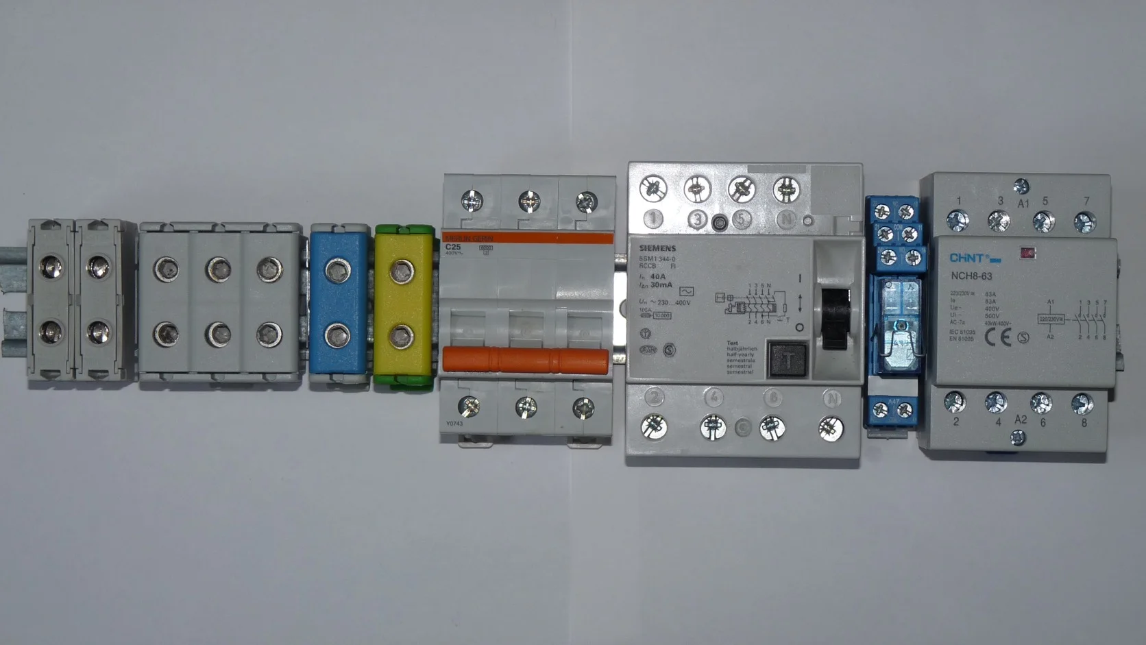
Hero photo: Components for DIN rail by Dmitry G, licensed under CC BY-SA 3.0. The original photograph was cropped and converted to WebP.
